Subtitles & vocabulary
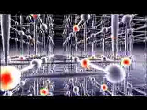
From sand to chip - How a CPU is made
00
alex posted on 2016/08/20Save
Video vocabulary

process
US /ˈprɑsˌɛs, ˈproˌsɛs/
・
UK /prə'ses/
- Transitive Verb
- To organize and use data in a computer
- To deal with official forms in the way required
- Noun (Countable/Uncountable)
- Dealing with official forms in the way required
- Set of changes that occur slowly and naturally
A2TOEIC
More journey
US /ˈdʒɚni/
・
UK /'dʒɜ:nɪ/
- Noun
- Act of traveling from one place to another; trip
- Intransitive Verb
- To travel through a place
A2TOEIC
More world
US /wɜrld /
・
UK /wɜ:ld/
- Noun (Countable/Uncountable)
- All the humans, events, activities on the earth
- Political division due to some kind of similarity
A1
More Use Energy
Unlock Vocabulary
Unlock pronunciation, explanations, and filters

