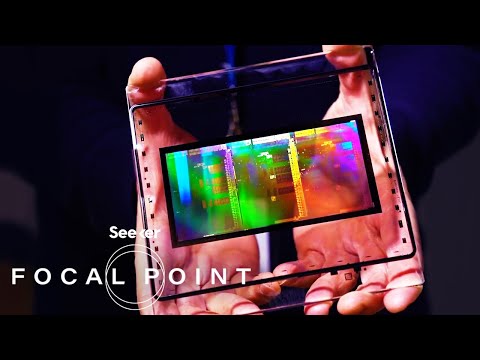
Subtitles section Play video Print subtitles We’re suiting up to take you inside a clean room that’s building an engineering marvel that’ll push the entire electronics industry to the next frontier. They're both amazing machines and scary machines. There's an enormous amount of complexity with them. There's an enormous number of things that can potentially go wrong. It's something that you don't necessarily sleep well at night, just having the machine on your floor. It’s about the size of a school bus, weighing over 180,000 kilograms, with over 100,000 parts, and 3,000 interlocking cables. Pop the hood and you’ll see lasers shooting tiny droplets of tin, generating plasma that’ll get collected and reflected by a series of mirrors, to then etch nanoscale patterns onto chips that’ll eventually go into your next cell phone. And after 30 years of innovations in physics, chemistry, and material science, it’s about ready for its debut. An integrated circuit, or chip, is one of the biggest innovations of the 20th century. It launched a technological revolution, created Silicon Valley, and everyone’s got one in their pocket. But if you zoomed in on one of those chips, I mean, really zoomed in, you’d find a highly complex, nanoscale sized city that’s expertly designed to send information back and forth. Semiconductor lithography is the ultimate alchemy, turning sand into gold. You start with the silicon wafer. You add insulators, add something called a gate which you apply a voltage to it, and it turns on or off the flow of electrons. That's the little switch that's sort of does the zero to one's that you always hear about You build up a sequence of layers. The network, the streets and buildings that you need in order to make these transistors and interconnect those transistors. At the end you can turn that into something that has substantially more value than a bucket of sand. At big tech conferences, chip manufacturers will announce they’ve hit impossibly small new milestones, like 22nm then 14nm and 10nm designs. That means they’ve found a way to shrink the size and increase the number of features on a chip, which ultimately improves the overall processing power. This is what’s been driving the semiconductor industry - a drumbeat called Moore’s Law. Moore's Law is an expectation. It's not a natural law. It's an expectation that we innovate at a pace of roughly doubling the density every two years. All of those things allow us to offer better products, allow us to offer cheaper products with the same capability and that in turn drives the demand for the overall industry. That means that we've got to be able to cram in, more and more functionality per square millimeter on a chip. All the designs and streets and everything have to be smaller and smaller in dimensions. Moore's Law has been predicted to be dying for a long time and yet it never is. Because each generation of engineers knows it's their expectation to keep working on it, to keep going at a certain pace. The core technique at the heart of this expectation is called photolithography. It’s a chip manufacturing process that’s similar to darkroom photography, but instead of a negative for a picture, they’re using something called a mask or reticle to expose a geometric print. It's basically a projection system where we have a light source, a mask or reticle, which is the blueprint, then the wafer. And we have to manage the light on the way through to get a perfect reproduction of that pattern on a silicon wafer. That enables you to build all of the billions of transistors that you need in order to make a functional chip. The light sources are lasers, created from a mixture of gases, like carbon dioxide or argon fluoride. When excited by an electric current, the gas molecules will emit laser radiation that are then tuned to a specific wavelength that imprints the chip design. There’s a drive to get the light source to shorter and shorter wavelengths, because the shorter it gets, the more transistors you can cram onto a chip. In terms of the electromagnetic spectrum, what we can see visibly is about 400 and 650 nanometers. The chip industry’s gone from 365 nm wavelengths to 248 nanometers to something called argon fluoride immersion. So argon fluoride refers to a wavelength, 193 nanometers. It is produced using a deep ultraviolet laser light source. The industry tried to go to 157 nanometer light, and that failed after companies had invested hundreds of millions of dollars in it. The field then had to invent new technical tricks for the systems in use today. They actually put water in between the bottom lens element and the wafer, because the wavelength of light in water is quite a bit shorter. When I first heard about it, I thought it was just crazy. You're going to get water all over the stages, and the electronics inside the tool. There was some very clever engineering that allowed them to contain that water in a little puddle as the wafer is going back and forth at about 700 millimeters a second. But that turns out to be coming near the end of its ability to produce even finer and finer features. So to keep Moore’s Law on track without breaking the laws of physics, chip manufacturers have been racing to bring this technology online: Extreme Ultraviolet Lithography. It takes the wavelength of light from 193 nanometers down to 13.5. The jump is much larger than what we would normally do. And that's partly because it's more of a disruptive technology. The first academic work on EUV was done in 1986, when I was still an undergraduate in college. Through my whole career, we've been hearing that EUV was coming. There was so many fundamental problems with using these soft x-ray wave lengths for a lithography tool. We're down to the point where the amount of variation can be measured in atoms. And so you have to work very hard to have a control of those dimensions. And that is where ASML comes in. ASML is the most important tech company you've never heard of. We build the big machines that make small chips. EUV was a massive step for us to undertake. Not only did we need to have an entirely new scanner because we had to work in a vacuum and at wavelengths where you need to have only reflective optics which required a huge amount of innovation. But we also needed a new light source as well. In fact, it's the first time ever, that we've needed to change the light source and huge elements of the scanner design at the same time. But for this story, we’re just going to focus on the lasers. Here’s how they work in the machine. The source of the light is a tiny little droplet of tin. They're smaller than the diameter of a human hair in which we fire across the vessel and then we intercept those with a pulsed laser beam of very high power. And I have to hit it with an accuracy of just a few microns even though it's traveling at, let me say at the speed in excess of the speed limit. It forms a plasma that emits EUV light. There's a collector mirror that collects that light and sends it into the scanner. Then there are four mirrors that essentially shape that light into a slit that bounces off the reticle. You will see a reticle stage doing this, and a wafer stage doing this. And what is happening is step and scan. Which basically means we continue to reproduce that particular pattern over and over again. Just to give you a sense of the mechanical complexity even, the wafer stage itself is something like 200 kilograms in weight and yet it's able to accelerate faster than a fighter jet. The thing that probably had people the most skeptical was, getting the power on the source up. When we started out we didn't generate the power that we wanted and we struggled at the beginning to understand why. Every year it was slipping out, and the actual power we were getting was stuck around very low levels, impractical levels. We continued to dive into looking more fundamentally at the basic plasma physics. What were we missing? It was around about 2015 where we finally unlocked the secret. It's all about exactly controlling how you deliver that energy to the droplet and then how you would deliver it to the tin afterwards. It becomes very critical in pushing that conversion efficiency up. You don't just need to hit the tin droplet with one laser pulse but, in fact, two. The first of those pulses, shapes the target in a way that enables us to get this high conversion efficiency and then the second pulse of course, generates that very hot plasma that we need for generating 13.5 nanometers at high power. Once we crested that, it became, I wouldn't say easy, but at least we saw the path and we were able to make changes to the system and we could see the immediate benefit. We actually still do work looking at how do we continue to push the power and the features of the light source that will support future scanners. Bunny suits are required around these precision tools, because the tiniest particle could kill a wafer pattern. The major source of particles in a clean room is actually the people. The equipment generally, unless something is actually scraping, something's misadjusted, they don't generate particles. The bunny suits are to protect the tools, and the wafers from the contamination. Here we have, largely the manufacturing activities as associated with the droplet generator. We also have an area we call integration where we look at the entire source and how it performs. When you go in to look at an EUV source, you see a large vessel with lots of interconnection everything. We have gas, power, water, etc. that's needs to be delivered. We'll see a beam transport system. So where we actually bring the high power laser beam into the vessel. ASML has been shipping this machine to chip manufacturers and it takes 40 freight containers, spread over 20 trucks and 3 cargo planes just to ship one of them. This is an army of people putting things together and pushing the edge of technology to make it work at all. And then of course having to make it work day in and day out.The EUV scanner is the most technically advanced tool of any kind, that's every been made. It's so far from normal human experience. I can't think of anything that has pushed the envelope in so many areas. There were many knowledgeable people in the field who just said. "You can never make a practical tool this way." We're just starting to enter into high volume manufacturing with EUV powered scanners and in fact, we're just starting to see some end products that are actually coming out that have chips that have been enabled by EUV technology. There's an insatiable amount of data, so you can build chips to store data, process data, move data around. The whole cloud is lots and lots of chips, doing all three of those things. I was talking with some people that are building the next particle accelerators and they're going to generate trillions of events every second. And there's no way to make sense of all of that even with this generation of computers. So you've got to go build ever faster computers, larger data storage, just to make sense of the science that's going on. Part of predicting the future is around diagnosing trends in technology. If you don't know what the future holds, are you afraid of that or are you encouraged by it? And I'm in the category of being encouraged by it because there's things to do that you haven't done before, things to create that you haven't created before. And then you may not set out to change the world, but we changed the world one step at a time.
B1 wafer chip light source moore law moore droplet The Extreme Physics Pushing Moore’s Law to the Next Level 20 3 林宜悉 posted on 2020/03/28 More Share Save Report Video vocabulary